 |
Add 32K on 16bit Bus
in Console |
This project is probably more difficult than most of the projects in this series. Not that anything is
that difficult to understand, it is more that there is a lot of soldering and steps to keep correct. For this
reason I have broken this major project into three smaller projects.
The first project is adding the RAM to the
console. This project is the largest of the three but gives the major result.
The second project will be adding
a switch which allows you to bypass the wait state defeat. This allows you to have 32K of RAM in
the console but it looks to the computer as if it is a memory expansion card. The reason for the switch is
so you can turn off the faster RAM for those programs which just might not like it.
The third project is adding LED's to show RAM access on either bus. This does nothing in it's self but I must
admit it looks pretty cool watching the reads. It also shows which programs use the VDP RAM (the 16k RAM that
came with the console) or the added 16bit RAM.
Don't let the number of instructions and pictures throw you. I put a lot of detail in this project to make it
as foolproof as I could. For some there is probably too much information, but I wanted to make sure that there
was enough information here for those who might be a little more nervous to try this project.
This project was created by Mike Ballmann and the instructions that I used for this project was described by
John Clulow. Part 2 of the project to bypass the 32/16-bit wait state was created by John Guion. The third
part of the project, adding the LED's was by Ron Reuter with help from John Creviston Jr.
|

|
|
Please make sure that all wiring and soldering is double checked before re-applying power. Though computer components are pretty hardy some do not take to being
wired up backwords or incorrectly. I have done my best to make sure that all diagrams
and instructions given here are correct, but I can not be responsible for any damage
an incorrect upgrade might cause. Also keep in mind that this will probably void any warranty :>).
|
The parts that will be needed for part 1 are as follows:
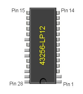
2 - 43256-LP12
1 - 74LS21
1 - 74LS153
The parts that will be needed for part 2 are as follows:
1 - 74LS08
1 - SPDT Switch
The parts that will be needed for part 3 are as follows:
1 - 5v LED
1 - 3v LED
1 - 74LS00
You will also need some very small gauge wire,
solder, and you will need a fine tipped soldering iron for this project.
Some good bright light, and a magnifier will help check for good solder joints.
|
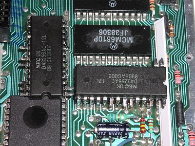
PART 1: Adding 32K to the Console

For a large picture view of the motherboard for part 1 go here.
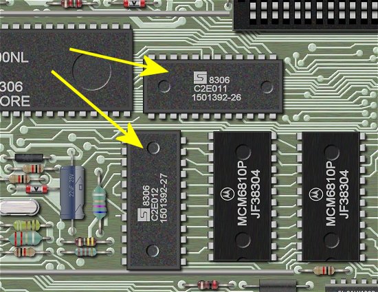
The first step (we are assuming you already have the motherboard laid out in front of you), is to prepare
the two 43256-LP12 RAM IC's. These will be piggybacked on top of the two ROM IC's. Be sure to bend the
pins of the RAM IC's in a bit so that they will fit snug against the pins of the ROM IC's. It was suggested
to use 28 pin sockets here. Feel free to do so, but my skills wouldn't allow me to get a soldering iron in
below the sockets.
The yellow arrows in the above graphic point to the TI's two ROM chips.
|
Next you will need to bend out certain pins on the 43256's. The above pictures shows which pins need to be
bent out. You do this to both IC's. The pins are: 1,2,20,22,23,26,27, and 28. These "bent" pins will NOT
be soldered to the ROM's.
|
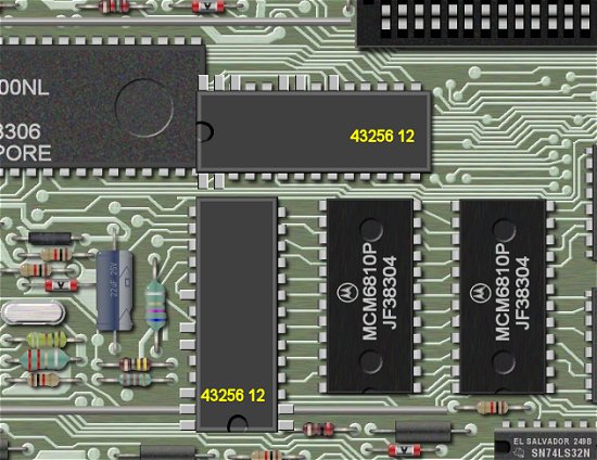
You are now ready to solder the RAM IC's to the ROM IC's. The above picture shows the placement of the IC's.
Notice the direction of the notches on the IC's. They point in the same direction as the notches on the ROM IC's.
You will also notice that RAM IC's are longer and have more pins than the ROM IC's. That is a good thing. The
RAM IC's will hang over the ROM IC's on the notched end. Pins 1,2 and pins 27,28 will extend over the ROM IC's.
In fact the RAM IC which is close to the TMS9900 IC will actually sit a little on top of the TMS9900.
Make sure that all the unbent pins fit snug against the pins of the ROM's. If they don't remove them and bend
in the pins a little more until they all fit snug. Be careful here not to run one of the pins in your finger!
Once you feel all the pins are snug you may start soldering all the unbent pins to the ROM's. Be careful here
that you don't bridge any solder, and that each of the pins are correctly soldered. When completed use a
magnifier and some good light to check all pins for good contact, and make sure nothing has been bridged by
the solder. As I described above there are some tight spots here, but it can be done. The picture below shows
a real picture of the installed RAM's.
|
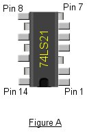
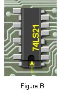
Next we will be working with the 74LS21 IC. On this IC bend out pins 1,2,4,5,6,8,10,12,14. Figure A above
shows the 74LS21 and the bent pins. Figure B shows how the 74LS21 will be piggy-backed on top of a 74LS138. Notice
that the 74LS138 is a 16 pin IC while the 74LS21 is a 14 pin IC. The un-notched end of the 74LS21 will line up
with the un-notched end of the 74LS138. Figure B shows this, and the small yellow arrows points to the end
of the 74LS21.
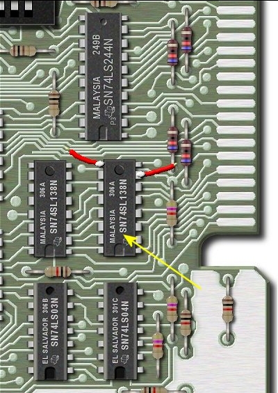
The picture below shows the location of the 74LS138 that the 74LS21 will be soldered to. Before soldering
The 74LS21 to the 74LS138 solder 1/2" lengths of wire to pins 7 and 9 of the 74LS138. This is much easier to
do now then after the 74LS21 is soldered on. The picture belows also shows these two wires soldered on to
the correct pins. Next solder all the pins that are not bent up of the 74LS21 to the 74LS138. Again check all
solder connections.
|
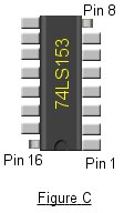
Our last IC in Part 1 is a 74LS153. Bend all pins up except for pins 8 and 16. Figure C above shows the
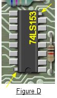
correct pins bent up. Figure D shows the 74LS153 piggy-backed on top of the 74LS194. The picture below shows where
the 74LS194 is located on the motherboard. Since both The 74LS153 and the 74LS194 are both 16 pin IC's they will
line up properly. Solder pins 8 and 16 of the 74LS153 to the pins 8 and 16 of the 74LS194. Figure D above shows
the two pins to be soldered by two small yellow arrows.
|
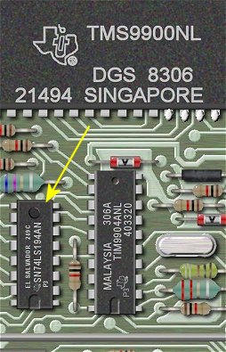
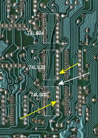
At the end of the TMS9900 (opposite to where you soldered the RAM's) you will find a line of three IC's. These
are a 74LS00, a 74LS32, and a 74LS04. The picture above shows the location of these three IC's on the
motherboard. Make note of roughly where these IC's are located and turn the motherboard over. We will need
to cut a trace which runs from pin 11 of the 74LS00 to pin 13 of the 74LS32.
The picture below shows where this is located on the back of the motherboard. The bottom yellow arrow is pointing
to pin 11 of the 74LS00, while the top yellow arrow is pointing at pin 13 of the 74LS32. The white arrow is
pointing at the trace, and where I cut it. Use an x-acto knife and carefully cut away about a 1/16" of the trace,
just make sure that you remove enough so that there is no longer any continuity between these two pins.
|
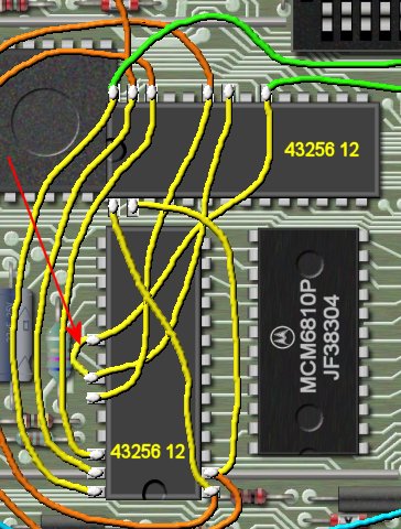
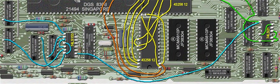
Now we are ready to solder some wires. The first thing we will do is solder wires to the 43256-LP12 RAM IC's.
Solder wires connecting every bent out pin on this RAM IC to the corresponding bent out pin on the other RAM IC.
Pin 1 to Pin 1, Pin 2 to Pin 2, etc. The picture above shows the all the wires soldered in place. All we are
concerned with at this point are the yellow wires in the above picture. Be sure to add the short piece of wire
as shown by the red arrow, which bridges pins 20 and 22. You only need to do this on the IC shown.
|
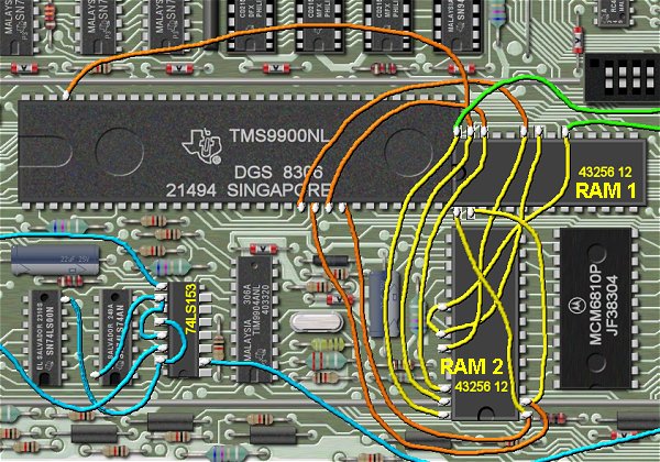
We will now solder some wires from the RAM to the TMS9900. You might wish to study the above picture to see where
all the wires go. At this point we are only interested in the orange wires. Also notice that I have labled the RAM IC's
as RAM 1 and RAM 2 for clarity.
From pin 1 on RAM 2 solder a wire which goes to pin 24 of the TMS9900.
Then solder a wire which runs from Pin 2 of RAM 2 to pin 22 of the TMS9900.
Next solder a wire to pin 23 of
RAM 1 to pin 21 on the TMS9900.
Pin 26 of RAM 1 goes to pin 23 on the TMS9900.
Next solder a wire from pin
27 of RAM 1 to pin 61 on the TMS9900.
|
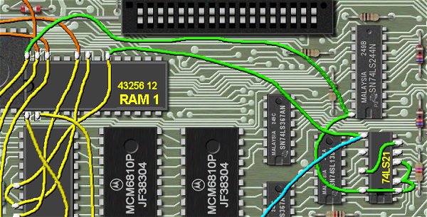
Now we will connect some wires to a 74LS244 and to the 74LS21 we added earlier. This is shown in the picture
above, and is shown by the green wires.
Solder a wire from pin 20 on RAM 1 to pin 8 on the 74LS21.
Next
solder a wire from pin 28 of RAM 1 to pin 20 of the 74LS244.
Now solder a wire to pins 1,2,4, and 14 of
the 74LS21.
Next solder the short wire (from earlier) from pin 7 of the 74LS138 (the IC that the LS21 is
piggy-backed on) to pin 5 of the LS21.
Next solder a wire from pin 6 to pin 12 on the LS21.
Now solder
the other short wire (from earlier) from pin 9 on the LS138 to pin 10 of the LS21.
Now solder a wire from pin 14
on the LS21 to pin 20 of the LS244.
OK!! we are almost finished. This would be a good time to take a break, and rest your eyes for a few minutes!
We don't want to get into a hurry now!
|
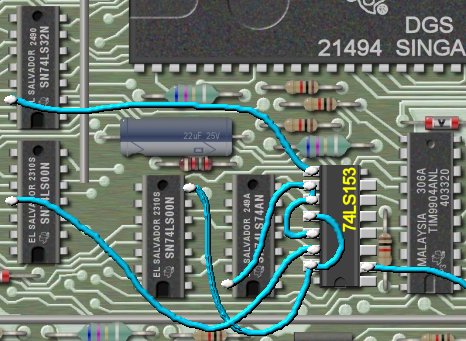
The above picture is a bit wide so you may need to scroll from side to side to see it all.
We will be refering to the blue wires in the above picture. The below picture shows a close up the
74LS153 and it's connections.
First solder a wire from pin 8 of
the 74LS21 to pin 2 of the 74LS153.
Connect pin 9 of the LS153 to pin 13 of the 74LS32.
Next solder
pin 10 of the 74LS153 to pin 14 of the 74LS74 which is right next to it.
Also solder another wire from
pin 10 of the 74LS153 to pins 11 and 13 of the 74LS153.
|
Now solder a wire from pin 12 of the 74LS153 to pin 15 of the 74LS153.
Next solder a wire from pin 15 of the
74LS153 to pin 7 of the 74LS00.
Here is the wire we have been looking for!
Solder a wire from pin 14 of the 74LS153 to pin 11 of the 74LS00.
|
At this point we are ready to test our work. Before you hook anything up, go over all the steps one more time
and compare your wiring to this diagram. Also check all solder joints
one more time, using a magnifier and a good light source. We don't want to release any smoke that is contained
in all electronic components.
I didn't want to re-assemble the console so I tested mine on my work bench using the seperate pieces. I hooked
up the keyboard, power supply, and cartridge port taking care that no parts where touching each other. Also
make sure where you set the pieces is very clean, and that there are no metalic pieces that could short one
of the parts. I also placed the cartridge holder into it's slot so I could insert the Extended Basic cartridge.
I have run motherboards for several minutes like this with no problems, but please note that you will do this at
your own risk. Keep in mind that the VDP chip (the one with the heatsink), can get very hot rather quickly, so
the whole point here is to have everything ready to go so that you only have the power on for a minute or so.
Turn the power on, choose extended basic. If the system does not come up or it makes any weird beeps,
immeditaly turn off the motherboard, and again check all wires, and solder joints.
At the prompt type size, you should see something like this:
"11840 BYTES OF STACK FREE, 24488 BYTES OF PROGRAM SPACE FREE"
If you do then turn off the motherboard, and pat yourself on the back!!
If this is as far as you wish to go then you can re-assemble the console.
If you wish to continue with part 2 then click here.
|
