 |
Add 32K on 16bit Bus
in Console Part 2
|
Bypassing the 32/16-Bit Memory
Conversion Wait State Defeat
The parts that will be needed for part 2 are as follows:
1 - 74LS08
1 - SPDT Switch (make sure switch is NOT center-off type)
You will also need some very small gauge wire,
solder, and you will need a fine tipped soldering iron for this project.
Some good bright light, and a magnifier will help check for good solder joints.
|

|
|
Please make sure that all wiring and soldering is double checked before re-applying power. Though computer components are pretty hardy some do not take to being
wired up backwords or incorrectly. I have done my best to make sure that all diagrams
and instructions given here are correct, but I can not be responsible for any damage
an incorrect upgrade might cause. Also keep in mind that this will probably void any warranty :>).
|
PART 2: Bypassing the 32/16-Bit Memory
Conversion Wait State Defeat
For a large picture view of the motherboard for part 2 go here.
This project will allow you to choose the option of using the 16-bit memory at the "regular speed". With
the switch in one position you will have the "fast" 16-bit RAM, while in the other position you will have
the standard 32K of RAM. This will be seen just like a memory expansion card in the PEB. This choice is to
allow you run any incompatible programs that might not run with "fast" RAM. With this switch you will not
need to switch consoles and then add 32K of RAM to the PEB.
This project was created by John Guion.
|

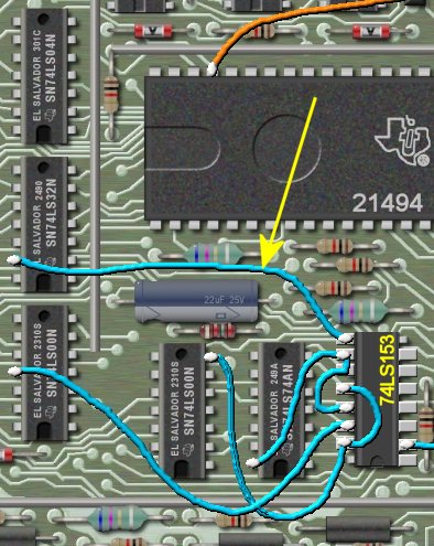
The first step will be to remove one wire which we soldered on the 74LS153 in part 1. The above picture shows
the wire which must be un-soldered from pin 9 of the 74LS153 and pin 13 of the 74LS32. This connection will NOT
be re-used.
|
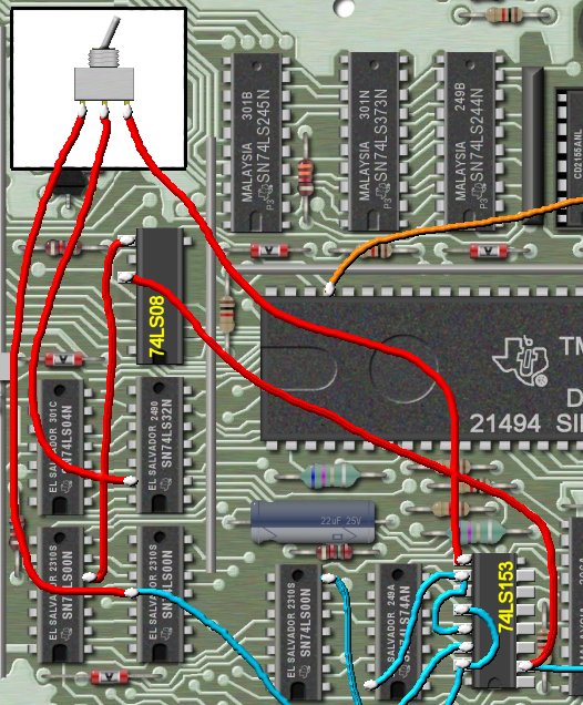
The next step is to determine where to mount the switch. That is really up to you. I mounted mine on top
of the case (see picture here). Just make sure you use enough wire to to be able to reach the switch when it
is mounted, while at the same time making the wires as short as you can.
For the wiring instructions in the above picture refer to the red wires.
The center terminal of the switch goes to pin goes to 13 of the 74LS32 where you removed the wire. Connect
one of the outer terminals of the switch to pin 11 of the 74LS00. Connect the other outer terminal on the switch
to pin 9 on the 74LS153 that you removed the wire from. Again, refer to the picture above.
|
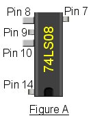
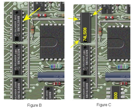
Take your 74LS08 and cut off all pins except, 7,8,9, and 10. See figure A above which shows the correct pins
to be left. Next bend out pins 8 and 10. Will be piggy-backing this IC on to the 74LS04. The location of
the 74LS04 IC is shown in figure B below. Place the 74LS08 on top of this IC with the notched ends lined up.
Solder pins 7,9, and 14 othe 74LS08 to the same pins on the 74LS04. The arrows on figure C below show the pins
that need to be soldered.
|
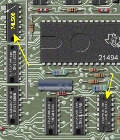
In this step we will be soldering a wire on the back of the motherboard. Make note of the two IC's shown
by the two yellow arrows above. One is the original 74LS04 with the 74LS08 we just soldered on. The other is
a 74LS194 with the 74LS153 piggy-backed on it. We will add the wire on the bottom of the motherboard since both
of this IC's have IC's stacked on them. The small white arrows show the the correct pins.
|
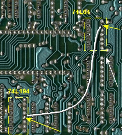
The above is an actual picture of the bottom of the motherboard showing the two IC's outlined in yellow. We
need to solder a wire from pin 9 of the 74LS04/74LS08 to pin 13 of the 74LS194/74LS153. The two yellow arrows
show these two pins.
Next we need to cut a circuit trace coming from pin 9 the 74LS04/74LS08. The white arrow in the above picture
shows where to cut the trace.
|
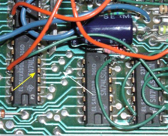
Our last step for this project is to cut one more trace on the top of the motherboard. The above picture shows
where this needs to happen. The yellow arrow shows pin 4 of the 74LS00, and the white arrow shows where to
cut the trace.
That's it! Again, check over all wiring and solder joints before testing the motherboard.
If you wish to continue with part 3 then click here.
|
