 |
TMS9918A VDP
|
The TMS9918A is the Video Display Processor (VDP) for the TI-99/4A. The TI-99/4 contained the TMS9918 (no A), and this
"A" is where the 4A got the "A" in its name. This was a powerful graphics chip and was used in several different
systems including the MSX.
|
KEY FEATURES OF THE TMS9918A | |
|
- 256 x 192 Screen Resolution
- 15 colors plus transparent
- Direct wiring to 4K, 8K, or 16K dynamic RAM memories
- Automatic and transparent refresh of dynamic RAMs
- Composite video output
- Unique planar representation for 3D simulation
- Standard 40-pin package
|

The 16 Colors
Color (HEX) | Color | | Color (HEX) | Color | | |
0 | Transparent |  | 8 | Medium Red |  | |
1 | Black |  | 9 | Light Red |  | |
2 | Medium Green |  | A | Dark Yellow |  | |
3 | Light Green |  | B | Light Yellow |  | |
4 | Dark Blue |  | C | Dark Green |  | |
5 | Light Blue |  | D | Magenta |  | |
6 | Dark Red |  | E | Gray |  | |
7 | Cyan |  | F | White |  | |
VIDEO DISPLAY MODES
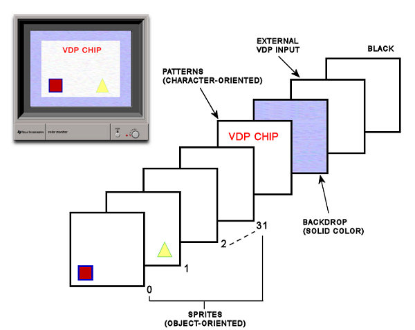
The VDP displays an image on the screen that can best be envsioned as a set of display planes sandwiched together. The
graphic above shows the definition of each of the planes. Objects on planes closest to the viewer have higher priority.
In cases where two entities on two different planes are occupying the same spot on the screen, the entity on the higher priority
plane will show at that point. The first 32 planes each may contain a single sprite. The areas of the Sprite Planes,
outside of the sprite itself, are transparent. Since the coordinates of the sprite are in terms of pixels, the sprite can be
positioned and moved about very accurately. Sprites are available in three sizes: 8x8 pixels, 16x16 pixels, and
32x32 pixels.
Behind the Sprite Planes is the Pattern Plane. The Pattern Plane is used for textual and graphics images generated by the
Text, Graphics I, Graphics II, or Multicolor modes. Behind the Pattern Plane is the backdrop, which is larger in area than
the other planes so that it forms a border around the other planes. The last and lowest priority plane is the External VDP
Plane. Its image is defined by the external VDP input pin which allows the TMS9918A to mix the external video signal
internal to the chip.
Graphics I Mode
In this mode the Pattern Plane creates 24 rows of 32 characters with each character being 8x8 pixels in size. Two
unique colors are allowed for each character. You can use any of the 16 colors, but only two
at a time can be used in a character. This mode gives the standard 32 column output of the TI-99. Sprites can be used
in this mode.
Text Mode
This mode creates 24 rows of 40 characters, with each character being 6x8 pixels in size. Sprites are not available in
this mode and only two colors can be defined for the entire screen. In other words you could have a blue background with
yellow text. This mode would only be useful with text only programs, but does permit 40 column output.
Multicolor mode
In this mode the screen is broken into a grid of 64x48 positions, each which is a 4x4 pixel. Sprites can be used in this
mode.
Graphics II Mode (bitmap mode)
This mode is similar to the Graphics I mode except that it allows a larger library of patterns. It has the same 24
rows of 32 characters, with each character being 8x8 pixels in size. The cool thing though, is that it segments the
screen into three equal parts, where as the Graphics I mode only can only use the first third of the screen. Sprites are
available in this mode.
|
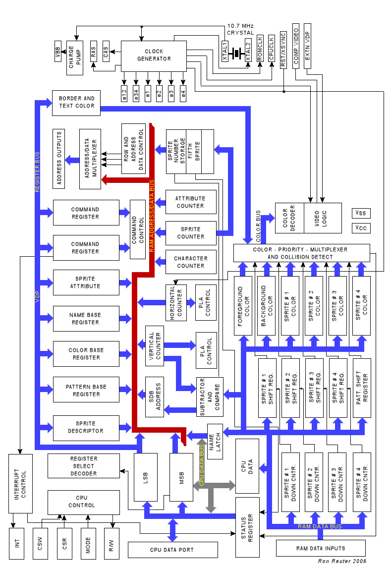
TMS9918A VDP BLOCK DIAGRAM
TMS 9918A PIN ASSIGNMENTS AND FUNCTIONS
SIGNATURE | PIN | I/0 | DESCRIPTION | |
XTAL1,
XTAL2 | 40,39 | I | 10.7+MHz crystal inputs | |
CPUCLK | 38 | O | VDP color burst frequency clock.
Typically not used on the TMS9918A | |
GROMCLK | 37 | O |
VDP output clock=XTAL/24. Typically not used. | |
COMVID | 36 | O |
Composite video output for the TMS9918A. | |
EXTVDP | 35 | I/O |
External VDP input. | |
RESET/
SYNC | 34 | I |
The RESET pin is a trilevel input pin. When it is below 0.8 volts, RESET initializes the
VDP. When it is above 9 volts, RESET is the synchronizing input for the external video. | |
VCC | 33 | I |
+5 volt supply | |
RD0 (MSB) | 32 | I |
VRAM read data bus. | |
RD1 | 31 | I |
VRAM read data bus. | |
RD2 | 30 | I |
VRAM read data bus. | |
RD3 | 29 | I |
VRAM read data bus. | |
RD4 | 28 | I |
VRAM read data bus. | |
RD5 | 27 | I |
VRAM read data bus. | |
RD6 | 26 | I |
VRAM read data bus. | |
RD7 | 25 | I |
VRAM read data bus. | |
CD0 (MSB) | 24 | I/O |
CPU data bus | |
CD1 | 23 | I/O |
CPU data bus | |
CD2 | 22 | I/O |
CPU data bus | |
CD3 | 21 | I/O |
CPU data bus | |
CD4 | 20 | I/O |
CPU data bus | |
CD5 | 19 | I/O |
CPU data bus | |
CD6 | 18 | I/O |
CPU data bus | |
CD7 (LSB) | 17 | I/O |
CPU data bus | |
INT | 16 | O |
CPU interrupt output. | |
CSR | 15 | I |
CPU-VDP read strobe | |
CSW | 14 | I |
CPU-VDP write strobe | |
MODE | 13 | I |
CPU interface mode select; usually a processor address line | |
VSS | 12 | I |
Ground Reference | |
R/W | 11 | O |
VRAM write strobe | |
AD0 (MSB) | 10 | O |
VRAM address/data bus | |
AD1 | 9 | O |
VRAM address/data bus | |
AD2 | 8 | O |
VRAM address/data bus | |
AD3 | 7 | O |
VRAM address/data bus | |
AD4 | 6 | O |
VRAM address/data bus | |
AD5 | 5 | O |
VRAM address/data bus | |
AD6 | 4 | O |
VRAM address/data bus | |
AD7 | 3 | O |
VRAM address/data bus | |
CAS | 2 | O |
VRAM column address strobe | |
RAS | 1 | O |
VRAM row address strobe | |
