 |
Geneve 9640
32K SRAM Upgrade
|
The following project appeared in the Nov/Dec 1998 MICROpendium and was written by Tim Tesch. I used the
instructions from his article and successfully added 32K of SRAM to allow me to run MDOS 6.0.
I found this project quite easy, and only took a few minutes to complete. Just be very careful, as you
are working with a piece of hardware that is getting quite hard to find.
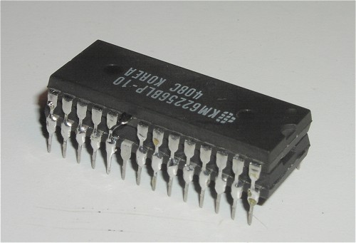
The only part you will need is a 62256LP-10 32K SRAM, and a piece of wire about 8" long. Several companies still make this chip
and mine happened to be a compatible manufactured by Samsung.
It is easy to check your card to see if it already has been upgraded without even removing
it from the PEB. Just boot your Geneve to mdos and type chkdsk. What you want to notice
is what is returned for the bytes of total memory. Without the upgrade it will read "557,056
bytes of total memory", with the upgrade it will read: "589,824 bytes of total memory".
If you card reports only 557,056 bytes of memory, then it is time to bring out the soldering iron!
|

|
|
"If you are not an experienced desolder/solder type then
let someone else do your repair/upgrade as the GENEVE board can be tough for
beginners as it is a three layer board". Geneves are very RARE, and every board COUNTS!
|

|
|
Please make sure that all wiring and soldering is double checked before re-applying power. Though computer components are pretty hardy some do not take to being
wired up backwords or incorrectly. I have done my best to make sure that all diagrams
and instructions given here are correct, but I can not be responsible for any damage
an incorrect upgrade might cause. Also keep in mind that this will probably void any warranty :>).
|
What we will be doing here is to remove an IC from it's socket, piggy back our 62256 IC on top
of the existing IC, replace the IC's back in their socket, and then solder one wire from the 62256 IC to the back of the Gate Array.
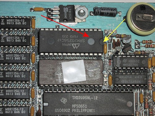
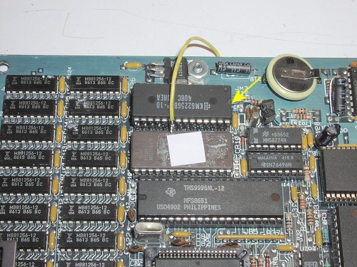
The above picture shows part of the Geneve motherboard. The red arrow is pointing at the IC (M87) that we
will be removing from it's socket. The yellow arrow is pointing at the "half moon" on the ic. When
replacing the IC's you must make sure that they are replaced with the "half moon" to the right as
shown in the above picture.
|
Gently pry the the noted IC out of it's socket. I DO NOT recommend that you solder on this chip while
still in the socket. Be careful when removing the IC that you do not bend any pins. We will be
re-using this IC. The best method is to "rock" the IC out of it's socket by prying a little on both sides until it is loose. Never pry
an IC out of it's socket by only prying on one side, this will result in bent pins!
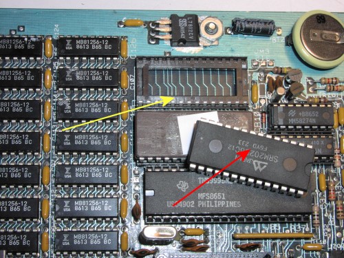
The yellow arrow is pointing at the now empty socket, while the red arrow is pointing at the removed
IC. "Look Ma!!! No bent pins!!"
|
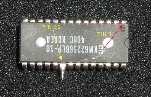
The above picture shows our new addition. This is the 62256 IC. Please note, that PIN 20 on this IC
must be bent up so it does not touch the pin on the IC we will be piggy backing it to. The yellow
arrow is pointing at this pin. The red arrow is just showing where PIN 1 is located for reference.
|
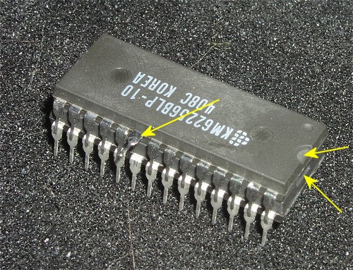
As you can see in the picture I have now piggy backed the NEW 62256 IC on top of the IC we removed
earlier. Make sure you line up the chips with both "half-moons" lined up. The two yellows arrows
point this out. Again note the yellow arrow pointing at PIN 20 which is bent out of the way.
We will be soldering a wire to this pin later in the project.
|
Now solder all pins except PIN 20 together. The above picture shows all the pins soldered. Use a
low wattage iron, and don't apply heat any longer then is needed. Also try to keep the bottom of the
pins on the original IC clean of solder as this IC will need to go back into it's socket.
|
Now place the IC's back in the socket that we removed the original from earlier. Again make sure that
you place the IC's in the socket with the "half-moons" pointing to the right as shown in the above
picture. Next solder a piece of wire (roughly 8" long) to PIN 20 of the new IC, and run it over the
board as we will be soldering the other end of the wire to the "back" of the motherboard.
|
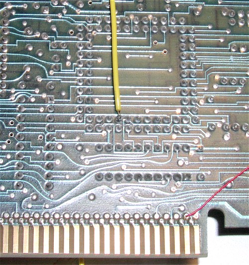
The above picture is showing the "back" of the Geneve motherboard. Solder the other end of the wire
(mine happens to be yellow) exactly where it shows in this picture, taking care not to bridge the solder
to any of the other pins.
This is the backside of the Gate Array IC (M86).
Now before we rush and plug the motherboard back into the PEB, let's double check our work.
Are the
IC's in the socket with the proper orientation?
PIN 20 is the one that is bent out, correct?
The yellow wire is soldered to the bottom, inside row, pin 5 from the left?
OK, let's test!
|
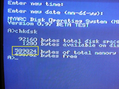
Place the motherboard back in the PEB. Hook up the keyboard and monitor cables. Turn on the monitor
and let it warm up. Power up the PEB, and boot to MDOS. When you're at a prompt, type chkdsk. You should
now see "589,824 bytes of total memory" as shown in the picture above.
As Tim Tesch stated in his article:
"Pat yourself on the back -- you've successfully modified your Geneve!
Go try MDOS 6.0!
|
